EMI – Electronagnetic Interference in industrial instalation and much more...

César Cassiolato
Marketing, Quality, Project and Services Engineering Director
SMAR Industrial Automation
cesarcass@smar.com.br
Introduction
The existence of equipment in different technologies combined with the inadequacy of installations facilitates the emission of electromagnetic energy, a fact that creates problems of elecromagnetic compatibility (EMC). See Figures 1 a and 1b, below.
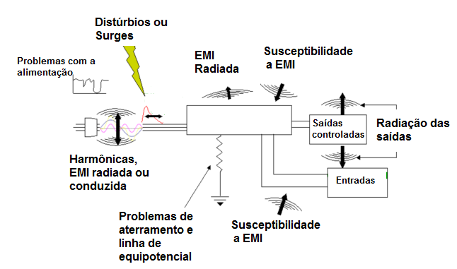
Figure 1 a – EMC sources
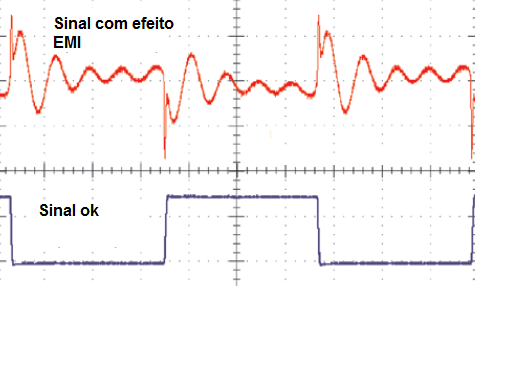
Figure 1b – Signal affected by EMI effects
See the electromagnetic spectrum on figure 2.
.png)
Figure 2 – Electromagnetic spectrum
.png)
Table 1 – Wavelength, frequency and energy for sellected areas of the electromagnetic spectrum
EMI is the energy that causes undesirable response to any equipment and can be generated by sparking on motor brushes, power circuit switches, activation of inductive and resistive loads, relay activation, switches, circuit breaks, fluorescent lamps, heaters, automotive ignitions, atmosphere discharges and even electrostatic discharges between persons and equipment, microwave sets, mobile communication equipment, etc. All of this can cause alterations and overvoltage, undervoltage, peaks, transients, etc. That may impact a communiction network. This is very common in the industries where EMI is very frequent in function of the larger use of machines (welding machines, for exammple), motors (CCM) and nearby digital networks and computers.
The biggest EMI problem is the sporadic situations that slowly degrade the equipment and their components. Most different problems can be generated by EMI, like in electronic equipment, with failure of communicton between devices of an equipment network and computers, alarms generated without explanation, action on relays, without logic or command, and burn down of components and electronic circuits. Power supply noises are very common due to poor ground and shield, or even project error.
Topology and wiring distribution, types of cables, protection techniques are factors to be considered to minimize the EMI effects. Remember that in high frequencies the cables behave like a transmission system with crossed and confusing lines that reflect energy and spread it from a circuit to another. Keep the connections in good conditions. Long-time innactive connectores may develop resistance or become RF detectors.
A typical example of how EMI can affect the behavior of an electronic component is a capacitor subject to a voltage peak higher than its specific nominal voltage. This may degrade the diolectric, whose thickness is limited by the capacitor operation voltage and cause a gradient of potential lower than the dialectric rigidity of the material and cause mal-functioning of or even burn the capacitor. It may also alter the transitors polarization currents, conducing them to saturation or cut, or even burn the components by joule effect, depending on the intensity.
Inadequate installations or the use of an equipment in non-recommended applications may harm a system performance and, consequently, the process performance, besides representing a source of danger and accidents. It is recommended, hence, the use only of trained and qualified professionals on installation, operation and maintenance services.
Very often the reliability of a control system is put at risk due to its bad installations. Commonly, users neglect their care, but more judicious analysis show problems on the installations involving cables and their routes and packaging, shields and grounds.
It is extremely important that everyone involved be aware and, mostly, committed to act with reliability, operational and personnal safety in a plant.
The control of noise in automation systems is vital, because it may become a serious problems even for the best devices and hardware of data acquisition and action.
Any industrial environment contains electrical noise in sources, including AC power lines, radio signals, machines and stations, etc.
Fortunately, simple devices and techniques, such as the use of adequate grounding methods, shielding, twisted pair wires, media signal methods, differential filters and amplifiers may control the noise on most measurements.
For example, frequency inverters contain commuting systems that may generate electromagnetic interference (EMI). They have high power commuting amplifiers that generate significant EMI on 10 MHz to 300 MHz frequencies. Certainly it possible that this commuting noise may generate intermitence in nearby equipment. While most manufacturers take due care in their projects to minimize this effect, the complet immunity is not feasible. So, some techniques involving layout, wiring, ground and shield contribute significantly to this purpose.
The reduction of EMI will minimize the initial costs and future working problems in any system.
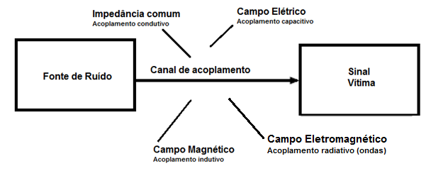
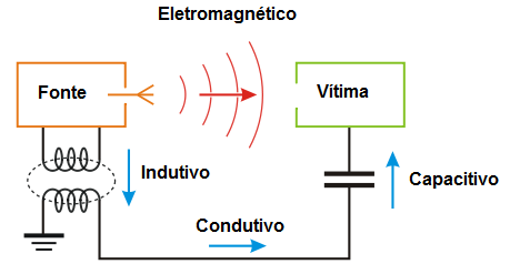
Figure 3 – Several coupling types generating noise in industrial installations
The signals may vary basically due to:
- Voltage fluctuation;
- Current harmonics;
- Conducted and radiated RF;
- Transitory (conduction or radiation);
- Electrostatic Fields;
- Magnetic Fields;
- Reflections;
- Crosstalk;
- Attenuations;
- Jitter (phase noise);;
- Etc.
The main interference souces – to be examined in detail are:
- Capacitive couplong (interaction of electrical fields betwenn conductors;
- Inductive couplong (followed by a magnetic field. The level of disturbance depends of the current variations (di / dt) and the mutual coupling inductance;
- Conduction through common impedance (grounding): it occurs when the current of two different areas pass through the same impedance. For example, the common ground way of two systems.
A few important points to understand EMC principles
There are some basic and important concepts to compare to better understand the effects of electromagnetic emission:
- Every AC signal at voltage or current level is real electromagnetic energy (Watts, Joules) propagated as wave.
- Electromagnetic waves are made up of electric field (E) and magnetic field (H).
- When a conductor is exposed to an electromagnetic wave, its free electrons move around it in response to this wave and generate current. This is called principle of reciprocity.
- The propagation of electromagnetic waves and associated fields are molded by the “accidental antennas” formed by their two-way current paths and that of the dielectric materials around it. The goal is project paths that minimize the accidental aerials, thus reducing emissions and increasing immunity.
- The return currents automatically take paths that minimize the total energy.
- Everything presents impedance to the electromagnetic waves.
An electromagnetic wave is a combination of an electric field and a magnetic field, which propagate on the same direction but in orthogonal plans. It is common knowledge that a variation of the magnetic field induces an electrical field and vice-versa, in that the electromagnetic wave of a magnetic field is generated by the magnetic field, which, on its part, is generated by the electrical field and both are nurtured in a perfect arrangement (see figure 4).
.jpg)
Figure 4 – Electromagnetic wave
· Furthermore, fields .jpg) and
and  are perpendicular to each other and also to the wave propagation direction, at a displacement with velocity v. This allows to classify the electromagnetic wave asatransversal wave. Figure 4 shows the arrangement of an electromagnetic wave electrical and magnetic fields, the direction of its propagation.
Types of interference
There are two types of interference, internal and external, continuous or intermittent. Each type has its own origin. The most common causes of continuous interference are:
- 50/60Hz Power Supply
- ElectricalMotor (Especially Commuter)
- Sinaisde rádio de alta energia
- High power radio signals
- Switching sources
- Microwaves
The constant noise causes are less difficult to identify than the problems with intermittent noises.
The most common noise source is constant, the one caused by a 50/60Hz power source. Power supply is the most common noise component because it is an oscillating voltage, has high power and a huge aerial system.
Almost every system has filters for 50/60 Hz, which may prevent or minimize this kind of noise.
Electrical motors very often create broadband noises that can propagate to any nearby equipment. DC motors frequently have switching sources that generate high frequency noise through the common ground. This broadband noise can be transmitted back through the power supply lines or through a common ground.
Local radio, television stations, radars and amateur radio stations can cause radio frequency noise.
These stations generate kW of energy and many times can be near industrial areas.
Commuted power supply is the most common source of noise. It is popular and a component of electroelectronic equipment. It creates huge quantities of harmonic frequencies.
The causes for intermittent noises are difficult to identify.
An example is a lightning, which can tipically contain 20 to 40 kA and million Volts. In addition, the lightning transmits broadband noise that covers the entire DC frequency spectrum. This, combined with the high voltage current, makes it impossible to filter the noise. The best method is protect the devices with shunts and suppressors.
Another common example in industrial ambients is relay commuting, which generally produces the relay commuting noise. This noise is created by the magnetic field when the relay is commuted.
The noise generated by welding machines is similar to a high frequency and broadband lightning noise. The difference is that it can be easily identified.
It is worth mentioning static noise (generated by static). It is very hard to be identified as a noise source, because it is invisible and very intermittent. Although many times created by Man, it can also originate from natural causes. Static noise is also similar to lightning noise with all its attributes, though in a smaller proportion.
Electromagnetic disturbances
Any electromagnetic phenomenon can degrade a system performance. Let us see some items related to these disturbances:
- Power supply voltage: during its distribution, it suffers a variety of disturbing effects. They could be caused by power supply network sources or by their users, or still by loads within an installation. Below are some typical of these disturbances:
- Interruptions
- Power drops
- Surges and Transients
- Distortions in wave form
- Amplitude and frequency variations
- Voltage Fluctuations
- DC in AC networks
- Electrical lines carrying signals
EMI causes and consequences
EMI consequences can be classified in different categories, depending on how critical they are.
Let us examine some EMI consequences:
- Failure of a critical safety item in machines and equipment
- Equipment irregular work
- A safety device may ignore a signal
- An operation may stop without apparent reason
- An equipment may have its intended function not executed in several situations, which runs unnoticed until a more serious situation turns into an accident.
.png)
Figure 5 – Real coupling situations
Capacitive Coupling
The capacitive coupling is represented by the interaction of electrical fields between conductors. A conductor runs close to a disturbing noise source, captures this noise and relays it to another part of the victim circuit. The capacitance effect between two bodies with electrical loads, separated by a dielectric is called mutual capacitance effect.
If the noise results from an electrical field, the shield actuation is effective, as Q2 cannot exist inside a closed and grounded enclosure.
.png)
Figure 6 – Q1 Load cannot create loads in a metal closed and grounded enclosure
An electrical field coupling is modelled as a capacitance between the two circuits (see figure 5). Figura 7 shows the physical model.
.png)
Figure 7 – Equivalent capacitive coupling circuit
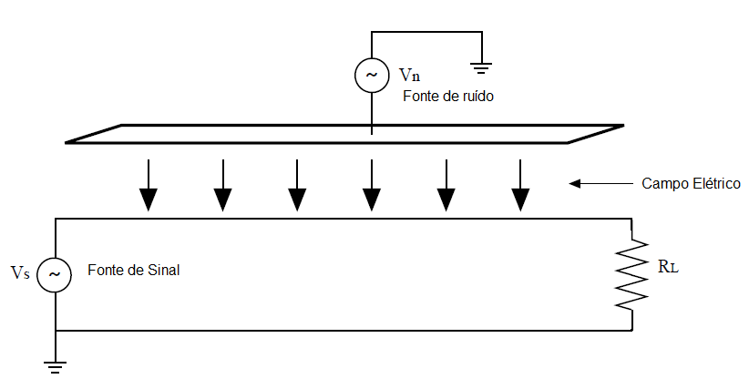
Figure 8 – Capacitive coupling physical representation
The equivalent capacitance, Cef, is directly proportional to the electric field actuation area and inversely proportional to the distance between the two circuits.
Therefore, by increasing the separation or reducing the area, the Cef influence will be minimized and, consequently, the capacitive coupling will affect less the signal. The capacitance effect between the two bodies with electrical loads, separated by a dielectric is called mutual capacitance effect.
The electrical field effect is proportional to the frequency and inversely proportional to the distance.
The disturbance level depends on the voltage variations (dv/dt) and the coupling capacitance value between the disturbing cable and the victim cable.
The coupling capacitance increases with:
- The inverse of the frequency: The potential for capacitive coupling increases as the frequency increases (the capacitive reactance, which can be considered as the capacitive coupling resistance, decreases according to the frequency and can be seen in theXC = 1/2πfC) formula.
- The distance between the disturbing and the victim cables and the length of the cables running in parallel
- The cables height in relation to the plan of reference (circuits with high input impedance are more vulnerable)
- The victim cable insulation (cable insulation εr), mainly for strongly coupled cable pairs.
Figures 9 and 10 show capacitive couplings examples.
.jpg)
Figure 9 – Capacitive coupling effect
.jpg)
Figure 10 – Example of capacitive coupling effect
Figure 11 shows coupling and its voltage sources and common mode and differential currents
.jpg)
Figure 11 – Capacitive coupling - Differential mode and common mode
Measures to reduce capacitive coupling effect
- Limit the length of the cable running in parallel
- Increase the distance between the disturbing cable and the victim cable
- Ground one of the shield ends of both cables
- Reduce the dv/dt of the disturbing signal by increasing the upward time
Whenever possible enclose the conductor or equipment with metallic material (Faraday shield). The ideal is that it covers one hundred per cent of the protected part and that this shielding do not act as a feedback or crosstalk element. Figure 12 shows the interference between cables, whose capacitive coupling between cables induces voltage transients (electrostatic pickups). In this situation the interference current is drained to the ground by the shield, without affecting the signal levels.
.png)
Figure 12 – Interference between cables: the capacitive coupling between cables induces voltage transient (electrostatic pickups)
.png)
Figure 13 – Cable interference: the capacitive coupling between cables induces voltage transient (electrostatic pickups) that may reach high frequency rates
.jpg)
Figure 14 – Capacitive effect in shieldless cable
.png)
Figure 15 – Alterations in upward and downward times
.png)
Figure 16a – EMI effect – Fake output transitions
.png)
Figure 16b – EMI effect on 4-20mA signal
On 4-20mA signals like in figure 16b, in some situations the noise is unnoticed, as it generally will affect the signal average, for example, and open one more valve, which implies losing process control efficiency or even in critical cases, such as fiscal measurements.
Figure 17 shows an example of protection against transients.
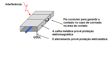
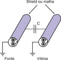
Figure 17 – Example of transient protection (best solution against Foucault current).
Electrostatic interferences can be reduced with:
- Adequate ground and shield
- Optical insulation
- Use of grounded metal channels and boxes
The influence can be minimized with the adequate use of the shield, which will act as a protection (Faraday cage). The shield must be placed between the capacitively coupled conductors and connected to ground at a single point, beside the signal source (see figure 19). Figure 18 shows an inadequate conditions, whose loop current circulates by the shield.
.png)
Figure 18 – Inadequate use of shield, grounded in more than one point.
.png)
Figure 19 – Adequate use of shield, grounded at a single point.
Inductive Coupling
The disturbing cable and the victim cable are accompanied by a magnetic field (see fiure20). The disturbance level depends on the current variations (di/dt) and the mutual coupling inductance.
.jpg)
Figure 20 – Inductive coupling – Physical representation and equivalent circuit
- The frequency: the inductive reactance is directly proportional to the frequency (XL = 2πfL)
- The proximity between the disturbing and the victim cables and the length of the cables running in parallel
- The cables height in relation to the reference plan (in relation to the earth)
- The cable load impedance or disturbing circuit
.jpg)
Figure 21 – Inductive coupling between conductors
.png)
Figure 22 – Example of Inductive Coupling noise
Measures to reduce inductive coupling effect between cables
- Limit the cables length running in parallel
- Increase the distance between the disturbing cable and the victim cable
- Ground one of the shield ends on both cables
- Reduce the dv/dt of the disturber increasing the signal upward time, whenever possible (resistors connected in series or PTC resistors on the disturbing cable, ferrite rings on the disturbers and/or victim cable)
.jpg)
Figure 23 – Cable-field inductive coupling
Measures to reduce inductive coupling effect between cable and field
- Limit the height h of the cable and the ground plan
- Whenever possible place the cable near the metal surface
- Use twisted pair cable
- Use ferrites and EMI filters
.jpg)
Figure 24 – Inductive coupling between cable and ground loop
Measures to reduce inductive coupling effect between cable and ground loop
- Reduce the cable height h and the cable length
- Whenever possible place the cable near the metal surface
- Use twisted pair cable
- In high frequencies ground the shield in two points (watch out!) and in low frequencies at a single point.
.jpg)
Table 2 – Distance between digital communication cables and other types of cables to ensure EMI protection
.png)
Figure 25 – Interference between cables: magnetic fields through inductive coupling between cables induce current transients (electromagnetic pickups)
Electromagnetic Interference can reduced with:
- Twisted cable
- Optical Insulation
- Use of metal grounded channels and boxes
To minimize the induction effect use the twisted pair cable that reduces the area (S) and diminish the Vb induced voltage in function of field B, by balancing the effects (average of the effects according to the distance):
.jpg)
The twisted pair cable is made up by wire pairs. The wires on one pair are coiled in spiral whose cancelling effect reduces noise and keep the electrical properties of the means constant through its entire extension. The reduction effect with the use of twisting has its efficiency in function of the flow cancellation, called Rt (in dB):
Rt = -20 log{(1/( 2nl +1 ))*[1+2nlsen(/nλ)]} dB ,
Where n is the number of loops/m and l is the cable total length (see figures 25 to 31).
The cancellation effect reduces the crosstalk between the wire pairs and decreases the level of electromagnetic/radiofrequency interference. The number of twists on the wires can vary to reduce the electrical coupling and their construction provides a capacitive coupling between the pair conductors and is more efficient in low frequencies (< 1 MHz). When it is not shielded, it has the disadvantage of producing noise in common mode. For low frequencies, i.e., when the cable length is smaller than 1/20 of the noise frequency wavelength, the shielding will present high noise susceptibility and in this case it should be grounded on both ends.
In the inductive caseVnoise = 2πBAcosα, where B is the field andα is the angle that the flow cuts the vector area (A) or still in function of the mutual M inductance:
.jpg)
.png)
Figure 26 – Inductive coupling effect in parallel cables
.jpg)
Figure 27 – Minimization of inductive coupling effect in twisted cables
.jpg)
Figure 28 – Examples of induction noise
(1).png)
Figure 29 – Example of induction noise
.png)
Figure 30 – Example of induction noise
.jpg)
Figure 31 – Example of Profibus cables near a power cable
Twisted pair cables are efficient as long as the induction in every tortion area be approximately equal to the adjacent induction. Its use is efficient in differential mode, balanced circuits, and has low efficiency in unbalanced circuits. In high frequency circuits with multi-points grounded the efficiency is high as the return current tends to flow by the adjacent return. However, in common-mode high frequencies the cable has little efficiency.
Capacitive and Inductive Coupling – Mutual Capacitance and Inductance in function of the distance between disturbing conductor and victim conductor
Both couplings are directly affected by the distance between the source of noise conductor and victim conductor. Next figure shows how they are affected depending of the distance between conductors.
.png)
Figure 32 – Mutual capacitance and inductance in function of the distance between the disturbing and the victim conductors
Coupling Modes
Some points deserve attention to better understand the EMI effects. There are differential-mode, common-mode and antenna-irradiated mode coupling concepts. They are applied to emission and interference coupling.
- Differential mode
In most cases, the desired signal is produced in differential mode. In the figure below, we have two equipment connected by on cable.
A radiated field can be coupled to this system and induce whatever interference in differential mode between both wires on the cable. By the same token, the differential current will induce its own radiated field. The ground plan does not play any role in this coupling.
- Common mode
The common-mode cable also transports common-mode currents on the same direction. These currents many times does not have any relation with the signal currents. They can be induced by an external field between the cable loop, the ground plan andthe different impedances.
The parasite capacitances and inductances associated with each equipment wiring and cabinet are components of the common-mode coupling circuit and play an important role in determining the distribution of amplitude and spectrum of the common-mode currents. These impedances are disperse and are not part of the equipment components and this is why their effects are difficult to control. Most certainly there techniques to minimize them.
.jpg)
Figure 33 – Radiated coupling modes
- Antenna mode
The currents in this mode are transported in the same direction by the cable and the ground reference plan.
They appear when the whole system (including the ground plan) is exposed to an external field. Currents generates via irradiated mode become a serious problem to the susceptibility of an irradiated field in independent systems when they are converted in currents of other modes (i.e., the differential or common mode), making the impedances vary on the different paths.
Transitories
Transitories and peaks are other examples of continuously generated EMI. They may be caused by electrostatic discharges (ES) or power switching. The figure below shows a transient typical curve.
Fast transitories can be coupled (mostly capacitively) in common-mode signal cables, especially if the cable is nearby or is located beside an impulsive interference source.
.png)
Figure 34 – Transient waveform
Power supply voltage variations
The power supply voltage may present a number of disturbances. The short duration voltage variation can affect definitely an equipment. They must be projected to minimize the effects on the following conditions:
- Short duration voltage drops
- Interruptions (complete lack of energy for more than 3 seconds)
- Harmonics and unbalance (voltage differences between phases)
- Flicker (fast voltage variations)
- Transitories
.png)
Figure 35 – Example of signal degradation due to harmonic
Electrostatic Discharge (ESD)
In this case, the probable coupling paths are:
- Insulation capacitance
- Connection and connecting junctions
- Wiring inductance due to magnetic fields generated in the discharge
Use of shieldng in inductive coupling
Magnetic shielding can be applied both to noise sources or signal circuits to minimize coupling.
Shielding low-frequency magnetic fields is not as easy as shielding electrical fields. The efficacy of magnetic shielding depends on the type of material and its permeability, its width and the related frequencies.
Due to its high relative permeability, steel is more efficient than aluminum and copper in low frequencies (less than 100 kHz).
In higher frequencies, however, aluminum and copper can be used.
The loss of absorption with the use of copper and steel for two widths is shown on figure 36.
.jpg)
Figure 36 – Loss of absorption with the use of copper and steel
The magnetic shielding in these metals is very efficient in low frequencies.
Skin Effect
In terms of shielding, an important feature is its depth(d)
This is the distance in the interiorof the material where the current density is reduced to1/e (0,37 or 8,7 dB), due to the peculiar skin effect. For eachddistance in the internal material direction, the current density drops 8.6 dB (around 9 dB). The bigger is the wall width, the bigger will be the attenuation of the current through it. This loss of absorption dependson the number of dthrough the wall. The d depth is an expression of the electromagnetic property that limits the AC current flow on a conductor surface, turning it smaller with the increase of conductivity, frequency or permeability.
.png)
Figure 37 – Skin (depth) of copper, aluminum and steel
The previous figure shows the depth (skin, d) of copper, aluminum and steel. For example, the aluminum depth at 30 MHz is 0,015 mm. This explains why fine conductors are effective in high frequencies: the current flow only at the surface and most part of the material does not affect the shielding properties. And still it is possible to reduce the current density from 18db in material with twice as much width (i.e, with three depth d layers) and so on. The requirements for an effective shielding are high conductivity for electric fields and high permeability for magnetic fields.
The skin effect leads to the conclusion thatthe AC resistance of a given conductor increases the the value of the current frequency that runs through this conductor.
In transient regime some points of interest deserve comment in that initially the current begins to establish itself on the conductor surface and later spreads to the center to produce an uniform current, noting that it initially has a high resistance and later, when it reaches the constant current, the resistance declines. The peculiar effect is more evident in high frequencies and the distribution of the current density is done exponentially, from the surface, material function and frequency.
Copper and aluminum have 5 times the conductivity of steel, being excellent to shield electrical fields with their relative permeability of 1 (the same as air). Carbon steel has great relative permeability around 300 at low frequencies, dropping to 1 with the increase of frequencies above 100 kHz. Its high permeability gives it a reduced ddepth and makes it better than aluminum for protection in low frequencies. Different types of stainless steel have different conductivity and permeability and, consequently, their ddepths may vary considerably.
A good shield material must have high conductivity, high permeability and enough width to reach the desired number of ddepth on the lowest frequency to be shielded. A width of one millimeter of steel covered with pure light zinc (around 10 microns) provides excellent protection for several applications.
Shield openings and efficacy
.png)
b) Shield efficacy x frequency
Simple Hole Several Holes
.png)
Figure 38 – Efficacy of shielding
Figure 38 shows how the shielding efficacy (SE) deteriorates with the frequency and the opening dimension. An opening of 100 mm will let pass around 20 dB more than a 10 mm opening. Openings are needed for access control, ventilation and interface, besides visualization. Discontinuity on the junctions between conductor elements also work as openings.
SE = 20log(l/2d)), where l is the wavelength and d is the largest opening dimension.
There is a number of variables that must be considered in relation to shielding efficacy:
- The shape, size, position and number of openings
- The relative positions and the distances between the noise source, the openings and the victim
- The shield geometry
- The frequency and impedance of the noise source
The shield material and shape will define how much of the incident electromagnetic wave will be reflected and absorbed, as well as how much will pass by the shield and reach the signal conductor wires. Mind also that the loss by absorption is defined as the relation between the shield width and its peculiar skin effect, which represents the wave depth of penetration contained in the interior of the shield. The largest the loss by absorption in dB, the better will the shield response.
A shielding efficiency, around 60 dB or more, provides very good level of protection. For a shielding to be efficient it is also necessary to evaluate the previously listed factors. Totally closed shields would be the ideal solution, as it would be much more efficient, but they are impractical. Shields are much more complex than a mere closed envelope made of metallic materials.
In the case of industrial installations, the shield, mainly on the junction boxes, is fundamental to keep the continuity and always keep the loop area the smallest possible on the stripped conductors. The shield connection at the ground point must be the smallest possible, as a connection of 30 cm would leave the shield with no effect for noises around hundreds of KHz.
.png)
Figure 39 – Behavior of an incident wave on the shield
The SE is normally limited by:
- Openings and junctions
- Removable covers
- Holes for control and display
- Holes for ventilation
- Holes for connectors
Openings and junctions mitigation:
- Minimize the size and number of openings and junctions
- Use junctions and seals to seal metal-metal interface
- Interface free of paint and debris
- Adequate coupling surface area
- Avoid galvanic corrosion
Metallic channel protection
Next let´s examine the use of metallic channels to minimize Foucault currents.
The spacing between channels facilitates the disturbance generated by the magnetic field. Furthermore, this discontinuity may ease the difference of potential between each channel segment, and in the case of a current surge, generated by atmosphere discharge or short circuit, for example, the lack of continuity will not allow the current to circulate through the aluminum channel, therefore without protecting the Profibus cable.
The ideal would be uniting each segment to the biggest possible contact area, which will provide better protection against electromagnetic induction and have between each segment a conductor on the channel sides with the smallest possible length, to ensure an alternative path to the currents, in case of occurring an increase of resistance on the junctions between the segments.
With the adequate mounting of the aluminum channel, the field, when penetrating in the channel aluminum board, produces a variable magnetic flow in function of the time [f = a.sen(w.t)] and originates an induced f.e.m. [ E = - df/dt = a.w.cos(w.t)].
On high frequencies, the f.e.m. induced on the aluminum board will be higher, originating a bigger magnetic field, which almost nullifies the magnetic field generated by the power cable. This cancellation effect is smaller at low frequencies. At high frequencies the cancellation is more efficient.
This is the effect of metallic boards and meshes when facing electromagnetic waves; they generate their own fields and minimize or even nullify the field through them and work as true shields to electromagnetic waves. They work as a Faraday cage.
Make sure the boards and coupling rings are made of the same material than the cable channels and boxes. Protect the connecting points against corrosion after mounting, with zinc paint or varnish, for example.
Although the cables are shielded, the shielding against magnetic fields is not as efficient as against electrical fields. In low frequencies, the twisted pair cables absorb most of the electromagnetic interference effects, while in high frequencies these effects are absorbed by the cable shield. Whenever possible, connect the cable boxes to the equipotential line system.
.png)
Figure 40 – Transient protection with metallic channels
Some observation relative to shielding:
- The cable shielding is used to eliminate capacitive coupling interference due to electric fields.
- The shielding only is efficient when establishes a low impedance path for the ground.
- A floating shielding does not protect against interferences.
- The shielding mesh must be connected to the circuit reference potential (ground) being shielded.
- Grounding the shield on more than one point may be problematic.
- Minimize the length of the reference-shield connection, as it works as a coil.
.jpg)
Figure 41 – The length of the reference-shielding connection must be minimized as it works as a coil.
- Electrical fields are much easier to shield than magnetic fields, and the use of shielding on one or more points works against electrical fields.
- The use o non-magnetic metals around conductors does not shield against magnetic fields.
- The key for magnetic shielding is to reduce the loop area, by using a twisted pair or the current return through the shield.
- To prevent conductor radiation, a shield grounded on both sides is generally utilized above the cut frequency, though under some precaution.
- Only a limited quantity of magnetic noise can be shielded due to the ground loop that is formed.
- Any shield through which a noise current flows must not be part of the signalpath.
- Use a shielded twisted pair or a triaxial cable in low frequencies.
- The efficacy of the twisted cable shield increases with the number of loops per cm.
Coupling by common or conductive impedance
It is the couplig by electric power transference through physical contact with a conducting means, in contrast with inductive and capacitive coupling. It may be via a wire, resistor, or a common terminal, transmission line, contact with the housing, grounding, etc.
The conductive coupling goes beyond the frequency spectrum and include DC. The interference occurs between the signal lines and the ground. The noise is caused by the existing resistance common to the signal and the return.
.jpg)
Figure 42 – Common ground and impedance
.png)
Figure 43 – Common ground and impedance
.png)
Figure 44 – Ground in series resulting in conductive coupling
The ground connection in series is very common because it is simple and economical. However, this is the ground that provides a dirty ground, due to the common impedance between the circuits. When several circuits share a ground wire, the currents on a circuit (that flow through the finite impedance of the common base line) may cause variations in the ground potential of the other circuits. If the currents are big enough, the ground potential variations may cause serious disturbances in the operation of all the circuits connected to the signal common ground.
.png)
Figure 45 – Common impedance
Measures to reduce the effect of conductive coupling between cables
Separate the ground power supplies and returns;
This type of coupled noise exists because the conductor have finite impedance. The effect can be elliminated or minimized by breaking the ground loops (if any) and enabling return to the ground. See Figure 46.
.png)
Figure 46 – Adequate ground and connections avoid conductive coupling
- Minimize common paths, especially high current, commuted currents and transient signals;
- On common paths always use the smallest resistance (for high currents) and the lowest impedance (for high di/dts);
- Use low impedance plans for DC sources and theirs returns. It is common to use a bypass capacitor between the source, keeping the high frequencies in theirs circuits.
Techniques to reduce conducted EMI effects
When the EMI manifests itself in relation to the conduction path, the following technical artifices can be used to:
- Reduce the EMI current and introduce high impedance elements in series;
- Conduct the EMI current to the ground, introducing low impedance elements in parallel;
- Block the EMI current, opening way with galvanic insulation elements;
- Neutralize the EMI current, using mutual inductance.
Some solutions based on galvanic insulation are effective for low and medium frequencies (below MHz). Solutions based on high frequency filters are effective in frequencies above MHz. See figure 47.
.png)
Figure 47 – Techniques to reduce EMI effects
Project and layout objectives in automation plants
One of the main goals in projects is to keep all common signal return points at the same potential. With high frequency in the case of inverters (up to 300MHz) harmonics are generated by the commuting amplifiers and in these frequencies the ground system looks more like an inductor and capacitor series than a low resistance path. The use of mesh and twists instead of wires (short wires are better for high frequencies) for connection at the grounding points are more effective in this case. See figure 51.
Another important goal is to minimize the magnetic coupling between circuits. This is generally obtained by minimum cable separation and cable segregated routing. The radio-frequency coupling is minimized by adequate shielding and grounding techniques. The transients (surges) are minimized with line filters and power suppressors on the colis and other inductive loads.
The grounding concept
A non-technical dictionary defines ground as a point in contact with earth, a common return in an electric circuit and an arbitrary point of zero voltage potential.
To ground or connect some part of an electric system or circuit to earth ensures personal safety and, generally improves the circuit work.
Grounding principles:
- All conductors have finite impedance that increases with the frequency;
- Two ground points separated physically are not in the same potential unless no other current flows between them;
- In high frequencies there is no single-point grounding;
- Unfortunately, a safe and robust ambient in terms of grounding, hardly happens simultaneously.
Ground wire
Every circuit must have a protective conductor through all its extension.
Sensitive Electrical Equipment Grounding
The grounding systems must execute several simultaneous functions: how to provide personal and equipment safety. In short, below is a list of basic grounding systems functions:
a) Provide personal safety to users;
b) Provide a low impedance return path (low inductance) to earth, and the automatic shutdown by the protection devices in a fast and safe way, when adequately designed;
c) Provide control to the voltages developed on the soil when phase-earth short circuit returns through the ground wire to a nearby or distant source;
d) Stabilize the voltage during electrical system transitories caused by ground faults;
e)Drain static loads accumulated on equipment structures, supports and housings in general;
f) Provide a system for the electronic equipment operate satisfactorily both on high and low frequencies;
g) Provide a stable voltage reference to signals and circuits;
h) Minimize EMI (Electromagnetic Emission) effects.
The neutral conductor is normally insulated and Power supply system used is the TN-S (T: point directly grounded, N: masses connected directly to the power supply point grounded, S: distinct conductors for neutral and for protection).
The neutral conductor basically conducts the system return current.
The protection conductor basically conducts the mass current to earth. All of housing must be connected to the protection conductor.
The equipotential conductor must work basically as a potential reference for the electronic circuit.
.jpg)
Figure 48 – TN-S system
To meet the above functions, three fundamental features are highlighted:
- Conduction capability
- Low resistance value
- Configuration of electrode to enable controlling the potential gradient.
- Regardless of having protective or functional finality, grounding must be single on each installation point. There are situation where the grounds can be separated, though under due precautions.
- Concerning the installation of the grounding system components, some criteria should be observed:
- grounding resistance value should not change considerably throughout time;
- components must resist to thermal, thermomechanical and electromechanical conditions;
- components must be robust or have adequate mechanical protection to meet the external influence conditions;
- damage to electrodes and other metallic parts by electrolysis effect must be prevented .
Equipotentialize
Definition: To place everything at the same potential.
In practice: Equipotentialize is to minimize the difference of potential to reduce accidents.
Each edification must receive a main equipotentializacion, and the installation located on the same edification must be connected to the main equipotentialization, hence to the same and only ground electrode. See figures 49 and 50.
Functional equipotentialization equalizes grounding and ensures good signal circuits work and electromagnetic compatibility.
Equipotentialization Conductor
- Principal – must have a minimum half protective conductor section of the bigger section and a minimum:
- 6mm2 (Copper);
- 16mm2(Aluminum);
- 50mm2(Steel)
.png)
Figure 49 - Equipotentialization
.jpg)
Figure 50 – Ground and Potential Line in Installations
.jpg)
Figure 51 –Equipotentializing Material
Considerations about equipotentials
Note figure 52, where there is a generating source of high tension and high frequency noises and a measuring system 25 m far from the control room, and, depending on the signal conditioning, there may be up tot 2.3kV on the measurement terminals. As long as shield, ground and equalization conditions improve, the ideal situation for measurement is reached.
.jpg)
Figure 52 – Example of how important are grounding and equipotentialization and their influence on signal
In distributed systems, like in industrial process control, whose areas are separated physically and powered by multiple sources, the rule is to have a ground system in each location and the EMI control techniques applied in each signal direction path, as shown on figure 50.
Implications of poor grounding
Inadequate or even bad grounding may impair more than just equipment safety. The main effects of inadequate grounding are electrical shocks to users by contact, slow (or intermittent) response from the protection systems (fuses, circuit breakers, etc.).
But also other operational problems may be caused by deficient grounding:
- Communication failures.
- Drifts or deviations, measurement errors.
- Excessive EMI generation.
- Abnormal heating on the power stages (inverters, converters, etc.) and motorization.
- Constantly stuck computers.
- Burn of electronic components without apparent reason, even in new and reliable equipment.
- Intermittence.
- Etc.
The grounding system must be unique and meet the following finalities:
- Electromagnetic interference control, both internal (capacitive, inductive and common impedance coupling) and external to the system (ambient);
- Operational safety, with the equipment housing connected to the protection ground and, therefore, any signal grounded or referenced directly or indirectly to the housing or to the panel, is automatically referenced to the power distribution ground;
- Protection against lightning, where the descending conductors of the System of Protection against Atmospheric Discharges (SPDA) must be connected to the metallic structures to avoid sparking, and ground electrode systems interconnected with the power ground, metal piping, etc., while the circuit ground stay connected to the lightning-rod ground, via structure or electrode system.
The consequence is that the equipment with metallic housings stay exposed to noise on the ground circuits (power and lightning).
To meet safety requirements, lightning protection and EMI, the ground system should be a zero-impedance plan, whose combination of different current levels would be free from interference. In other words, this is an ideal condition, which, however, is not confirmed in practice.
Types of Ground
In terms of process industry, some types of ground can be identified:
-
“Dirty ground”: Those present on installations typically involving 127VAC, 220VAC, 480VAC associated to high commuting level, such as CCMs, lighting, power distribution, EMI generating sources etc.
-
It is common that AC primary power supply present peaks, surges, spikes that degrade the AC ground.
-
“Clean ground”: Those present on typically 24VDc DC systems and circuits, powering PLCs, controllers and having aquisition and data control signals, as well as digital networks.
-
“Structural ground”: Those applied via structure that force the signal to 0V. They tipically work as Faraday cage in protection against lighting.
Note: “chassis” or “housing” ground is used as electric shock protection. This type of ground is not a “zero resistance” ground and its ground potential may vary. However, the circuits are almost always connected to the earth to prevent shock risks.
Single-point ground
This system may be seen on figure 53, where the striking feature is a single ground point distributed to the entire installation.
.png)
Figure 53 – Single-point ground
This configuration is most adequate for low-frequency spectrum and also meets perfectly well the needs of high frequency electronic systems installed in small areas.
Furthermore, this system must be insulated not to work as return path for signal currents, which should circulate through signal conductors with balanced pairs, for example.
This parallel grounding eliminates the problem of common impedance, although being detrimental to a big pile of cabling. In addition, the impedance on each wire can be too high and the ground lines can become sources of noise to the system. This king of situation can be minimized by choosing the right conductor type (AWG 14). Cables of larger gauges help reduce the ground resistance, as long as the flexible wire reduces the ground impedance.
Multipoint ground
For high frequencies, the multipoint system is the most adequate, as shown on figure 54, inclusive by simplifying the installation.
.png)
Figure 54 – Multipoint grounding
.png)
Figure 55 – Grounding in Practice
Multipoint ground systems that use balanced circuits do not show noise problems. In this case, the noise is filtered and its field is kept between the cable and ground plan.
.png)
Figure 56 – Inadequate multipoint grounding
.png)
Figure 57 – Adequate single-point ground
(1).png)
Figure 58 – Degradation on single-point grounding with interconnections and parasitic capacitances.
Figure 57 shows an adequate ground whose individual currents are conducted to a single grounding point.
Serial connection to ground is very common because it is simple and economical. However, this grounding provides a dirty ground, due to the common impedance between the circuits. When several circuits share a ground wire, the currents on a circuit (flowing through the common finite impedance of the base line) can cause variations on the ground potential of the other circuits. If the currents are large enough, the ground potential variations can cause serious disturbances in the operations of all the circuits connected to the common signal ground.
.jpg)
Figure 59 – Inadequate, weather-exposed ground, oxidation and increase of impedance on the ground contact put the system at risk.
Modern electronic systems rarely have only one ground. To mitigate the interference, like the common-mode impedance coupling, etc., distinct aspects on each sub-system by structural reasons, protection areas and foundations of primary and secondary power are desirable, in addition to the economical and logistic aspects involved. Finally, these individual points on each sub-system are connected to the single ground system, where there is the total potential reference of the system. See figure 60.
.png)
Figure 60 – Grounding Hierarchy
Grounding loops
A grounding loop occurs when there is more than one grounding path, generating undesirable currents between these points.
These paths form the equivalent to an antenna loop that captures interference currents with high efficacy.
Hence, the voltage reference gets unstable and the noise appears on the signals.
.png)
Figure 61 – Ground loop
.png)
Figure 62 – PROFIBUS-DP and grounding loops
Grounding at equipment level: Practice
In practice, there is a “mixed system” separating similar circuits and segregating them according to noise level:
- “signals ground” for more sensitive circuits;
- “noise ground” for commands (relays), high power circuits (CCMs, for example);
- “equipment ground” for racks, panels, etc.
.png)
Figure 63 – Grounding at equipment level in practice
The signals may vary basically due to:
- Voltage fluctuation
- Current harmonics
- Conducted and radiated RF
- Conduction or radiation transitories
- Electrostatic Fields
- Magnetic Fields
- Reflections
- Crosstalk;
- Attenuations
- Jitter (phase noise)
- Etc.
Field Equipment Grounding
The great majority of field equipment manufacturers, such as pressure, temperature transmitters, positioners, converters, etc, recommends local grounding for their products. It is common that their housings have one or more ground terminals.
When installed, the equipment housing is in contact with the structural part or piping and, consequently, grounded. If the housing is isolated from any structure point, local grounding is recommended with the shortest possible connection with AWG 12 wire. In this case, be careful in relation to the difference of potential between the grounded point and the panel where the controller (PLC) is installed.
Some makers recommend that the equipment floats, i.e., be isolated from the structure and not be grounded, thus avoiding current loops.
In relation to the classified areas, it is recommended to consult local regulations.
For micro-processed, digital communication equipment, some producers incorporate or enable surge or transient protectors. They provide protection against peak currents and a low impedance path to the grounding point.
General tipos involving control panels, CCMs and instrumentation
- Use RFI filter and always connect it the closest possible to the noise source, between the filter and the drive.
- Never mix input and output cables.
- All the motors activated by inverters must be powered preferably with shielded cables grounded on both ends. This is recommended by all inverter manufacturers. Remember that the commutation frequencies vary from 1k to 35KHz, normally 30KHz, which greatly influences the FF and the Profibus-PA.
- Whenever possible use an insulating transformer to power the automation system.
- Use repeaters on galvanically insulated CCMs, thus avoiding grounding differentials.
- To comply with EMI protection requirements all external cables must be shielded, except network powering cables. The shield circuit must be continuous, without interruption.
- Make sure that cables on different zones are routed in separate ducts. Inside the panel, create distinct zones even with separating plates previously used as shield.
- Make sure that the cables cross each other at square angles to minimize couplings.
- Use cables with the lowest possible values of impedance transference.
- On control cables install a100 nF to 220 nF small capacitor between the shield and the ground to prevent AC return circuit to ground. This capacitor will work as interference suppressor. But always refer to the inverter manuals.
- Choose toroid inverters or add toroids (common-mode choke) on the inverter output.
- Use 4-paths insulated and shielded cable between the inverter and the motor and between the power supply system and the inverter.
- Always ground the motor housing. Ground it on the panel, where the inverter is installed or on the inverter.
- Line reactors are a simple and inexpensive way or increasing the insulated load impedance source (as a variable frequency command, in the inverters case).
- The reactors are connected in series to the harmonic generating load and when increasing the source impedance, the magnitude of the distorted harmonic can be reduced to the load in which the reactor is activated. Consult the inverter manual and check the recommendations.
- The ideal is to embed the input inductor and RFI/EMC filter to work as an additional protection for the equipment and a harmonic filter for the electric network where it is connected.
- The main function of the RFI input filter is to reduce the radio-frequencies emissions conducted to the main distribution lines and to the ground wires. The RFI input filter is connected between the AC input power supply line and the inverter input terminals.
- Reflected waves: if the used cable impedance does not match that of the motor, there will be reflections. Remember that the cable between inverter and motor presents impedance to the inverter output pulse (the so-called surge impedance). In these cases reactors are also recommended.
- Special cables: another important detail that helps minimize the effects of electro-magnetic noises generated in installations with AC inverters and motors is the use of special cables that avoid the corona effect of discharges that can deteriorate the insulation dielectric rigidity and allow the presence of stationary waves and the transference of noises to the ground web. Another construction feature of some cables is double shield, which is more efficient as EMI protection.
- In terms of digital networks, keep it away from the inverter, where signals reach the motors and install repeaters to isolate de areas.
- Check for the need to ……. (?)the common-mode inverter capacitors on the DC bus.
- The cable gauge specifications and other recommendations are generally based in 75ºC. Do not reduce the wire gauge when using higher temperature wire. The minimum and maximum gauges depend on the inverter nominal current and the terminal blocks physical limitations.
- The ground connectors must be classified according to the inverter maximum current capacity.
- For inverter AC variable frequency applications that must comply with EMC standards, use the same type of shielded cable specified for AC motors between the inverterand the transformer
- Keep the motor cable lengths within the limits established by the inverter user manual. Many problems may occur, including on the cable load current and the wavelength voltage effort. Discreet I/O as on startup and shutdown can be connected to the inverter with several cables. The cable shield is recommended, as it helps reduce crossed coupling noise on power supply cables. Standard individual conductors compliant to general temperature, gauge and applicable codes specs are acceptable, provided they are distant from high voltage cables, to minimize noise coupling. However, multi-conductor cables could be less expensive.
- Pay attention to cables insulation, normally those higher than 300V.
- For multiple motor applications, chech carefully the installation. Generally, most installations do not show problems, although load currents on high peak cables may cause over-currents on the inverter or failures on ground.
- If there are TE and PE terminals, ground them separately at the closest panel point using twisted pair mesh. If using a panel PE ground wire, it must be connected onthe same panel side as the channel/armor connections. This will keep the common-mode noise away from the PLC backplane.
- Cable shielding:
- Motor and input cables
- Motor and input cable shield must be connected on both ends to provide continuous path for common-mode noise current.
- Control and signal cables
- The control cable shield must be connected at a single end only. The other end must be cut and isolated.
- The cable shield between two cabinets must be connected to the signal-source cabinet.
- The cable shield between a cabinet and an external device must be connected on the cabinet end, unles otherwise specified by the external device maker.
- Never connect the shield on the common side of a logic circuit, as it will bring the noise to the logic circuit. Connect the shield directly to the rack shield.
- When directing the wiring to the inverter, separate the high voltage wires and the conductors of the I/O motor and signal conductors motor. To keep them apart, direct them through a separate channel or use box dividers.
- Do not direct more than 3 sets of motor conductors (3 inverters) through the same duct. Keep the duct filling limits compliant to the applicable electricity codes. Do not pass motor conductors or power supply or communication cables through the same duct. If possible, avoid directing large lengths of input power supply wires and motor conductors by the same duct.
- As to boxes (trays), arrange carefully the geometry of multiple cable sets. Keep the conductors on each group in the same package. Arrange the conductors in a way that minimizes the induced current between the sets and keep them balanced. This is critical in inverters with nominal power of 200 HP (150 kW), in addition to keeping the power supply and control cables separate. When arranging the cable boxes for large inverters, check if the tray or duct containing the signal cabling is at 30cm or more apart from the one containing the motor or power supply wiring. The electro-magnetic fields of the motor or power supply currents may induce currents on the signal cables. The dividers also provide excellent separation.
- Make the connections ends for the inverter power supply, motor and terminal blocks control.
- On low frequencies, CC levels up to 1 MHz, the cable shield can be grounded at a single cable end and provide good response in relation to electromagnetic interference. On high frequencies, the recommendation is to shield the cable at both ends. In these cases, it is very important that the ground potential differences on both grounding connection points be the minimum possible. The voltage difference between both ends must be a maximum of 1 V (rms) to minimize the ground loop effects. Also important is to consider that high frequencies carry parasite coupling capacitance that tends to complete the loop when the shield is grounded on a single cable end.
Shielding on classified areas
Always verify the NBR 5418 standard for shielding and the connection with the equipotential system of intrinsically safe systems.
An intrinsically safe circuit must float or be connected to the equipotential system associated with the classified area only on a single point.
The insulation level required (except on one point) must be projected to support 500 V on the insulation test in compliance with 6.4.12 of IEC 60079-11.
If this requirement is not met, the circuit should be considered as grounded at that point. More than one ground connection is allowed on the circuit, provided that the circuit is divided in sub-circuits galvanically insulated and each one is grounded at a single point.
Shields must be connected to ground or to the structure, compliant to ABNT NBR IEC 60079-14.
Whenever possible, connect the cable boxes to the equipotential line system.
The shields must be grounded on a single point on the potential equalization conductor. If necessary, for functional reasons, small ceramic type capacitors (below 1 nF and for 1500V) are allowed to be installed as other grounding points, as long as the total capacitances do not exceed 10 nF.
Never install a previously installed device without an intrinsically safe system, as the protection zener may be burned and will not work properly on intrinsically safe areas.
Grounding and shielding cautions and recommendations for PROFIBUS-PA and Foundation fieldbus bus
When considering the use of shielding and grounding on field buses, take into account:
- The electromagnetic compatibiliy (EMC).
- Protection against explosion.
- Protection of persons.
Compliant with the IEC 61158-2 spec, to ground means to be permanently connected to earth through a sufficiently low impedance and sufficient conduction capacity to prevent any voltage that might result in equipment or personal damages. Voltage lines with 0 Volt must be connected to the ground and galavanically insulated from the fieldbus bus. The purpose of grounding the shield is to avoid high frequency noises.
Preferably, the shield must be grounded on two points, at the beginning and the end of the bus, as long as there is no potential difference between these two points, allowing the existence of loop current paths. In practice, when this difference exists, it is recommended grounding the shield at a single point, i.e., or the power supply or the intrinsic safety barrier. The continuity of the cable shield must be ensured on more than 90% of the total cable length.
The shield must completely cover the electric circuits through connectors, couplings, splices and distribution and junction boxes.
Never use the shield as signal conductor. Always check the shield continuity until the last field equipment segment and analyze the connection and finishing, as the latter must not be grounded on the equipment housing.
On classified areas, if it is not feasible the potential equalization between the safe area and the hazardous area, the shield must be connected directly to the ground (Equipotential Bonding System) only on the dangerous area side. On the safe area, the shield must be connected through a capacitive coupling (preferably a dielectric solid ceramic capacitor), C<= 10nF, insulation voltage >= 1.5kV).
.jpg)
Figure 64 – Shield + Ground Ideal Combination
Safe Area Potentially Explosive Area
.png)
Figure 65 – Capacitive Grounding
The IEC 61158-2 standard recommends complete insulation. This method is used mainly in the US and the UK. In this case, the shield is isolated from all grounds, except on the negative souce ground point or the intrinsic safety barrier on the safe side. The shield must be continuous since the beginning of the segment, passing by the junction and distribution boxes and reach the equipment. This method has the disadvantage that it does not protect totally the high frequency signals and can generate communication intermittence, depending on the cable topology and length. In these cases, the use of metallic channels is recommended.
Another complementary way would be to ground the equipment junction boxes and housings on a ground equipotential line on the non-safe side. These grounds are separated from the safe side ones.
Multiple-ground condition is also common, providing more effective protection on conditions of high frequency and electromagnetic noises. This method is adopted in Germany and some European countries. The shield is grounded on the source negative ground point or on the safe side intrinsic safety barrier and, additionally,on the ground of the junction boxes and the equipment housing. These are also grounded on the non-safe side. Another complementry condition would be grounding the ground wires in equipotential lines set, bonding the non-safe to the safe side.
For more details, always consult the local safety regulations, Use the IEC 60079-14 standard as a reference on classified areas applications.
Figures 66 and 67 show the shield on adequate and inadequate grounding conditions.
.png)
Figure 66 – Inadequate fieldbus shield grounding on more than one point.
.png)
Figure 67– Adequate fieldbus shield grounding on a single point.
Shielding
Grounding and shielding are mandatory requirements to guarantee the integrity of a plant data. In practice is fairly common to encounter intermittent work and crude measurement errors due to poor installations.
Noise effects can be minimized with adequate project techniques, installations, grounding and shielding, cable distribution. Improper grounding can be the source of undesirable and dangerous potentials that can jeopardize an equipment effective operation or a system performance.
The shield must be connected to the reference potential it protects (see figure 68)
.png)
Figure 68 – Shield connected to the signal reference potential it is protecting
With multiple segments, keep them connected to ensure the same reference potential, according to figure 69.
.png)
Figure 69 - Multiple segments connected to the reference potential it protects.
Shielding x grounding effect on a single point
In this case the current will not circulate through the shield and does not cancel magnetic fields.
The conductor length projected beyond the shield must be minimized to ensure good shield connection to the ground.
.jpg)
Figure 70 – Shielding x grounding effect on a single point
Shielding x grounding effect on two points
A current distribution occurs in function of the frequencies, as the current tends to follow the path with the least impedance.
Up to a few kHz, the inductive reactance is negligible and the current will circulate through the path with the least resistance.
Above kHz, the inductive reactance predominates and the current will circulate through the path with the least inductance.
The path with the least impedance is that whose return course is near to the departure course, as it presents the largest distributed capacitance and the least distributed inductance.
The conductor length projected beyond the shield must be minimized to ensure good shield connection to the ground.
.jpg)
Figure 71 – Shielding x grounding effect on two points
It is worth mentioning in this case:
- There is no protection against ground loops.
- Possible significant damage to active equipment when the ground potential between the extremes exceeds 1 V (rms).
- The electrical grounding resistance must be the lowest possible on both segment ends to minimize ground loops, mainly on low frequencies.
As previously seen, cable shielding is used to eliminate capacitive coupling interference due to electrical fields.
Conclusion
This article showed several details on inductive/conductive capacitive coupling effects, as well as details on grounding.
Every automation project must take into account standards that ensure adequate level signals, in addition to the safety required for the application. Bear in mind that adequate, standard installations are the basis for success of a digital technology project.
Mitigation of EMC questions:
- Reduce interference levels generated by EMI sources disturbing points
- Increase the victim susceptibility (immunity)
- Reduce the efficacy of coupling paths and the following combination:
|
Disturbing (EMI) source |
Coupling path |
Victim |
|
Alteration of signals routing |
Increase the separation |
Alteration of signals routing |
|
Add local filters |
Shielding |
Add local filters |
|
Select the operation frequency |
Reduce the number of interconnections |
Select the operation frequency |
|
Frequency dithering |
Filter interconnections |
|
|
Reduce the signal level |
|
|
Table 3 – Measures to mitigate EMC
.png)
Figure 72 – How to minimize EMI effects
Preventive maintenance should be executed annually, by checking the quality of each connection in relation to robustness, reliability and low impedance, making sure that there is no contamination or corrosion. In addition, digital technology plants such as Profibus and Foundation fieldbus, should only have network certification service provided by trained professionals, to ensure conformity with standards in addition to advantages like:
- increased network performance and reliability;
- reduction of comissioning, startup and shutdown time;
- preventive and predictive actions on possible installations and communication signals failures;
- increase of operational safety with the suggested improvements;
- improvement of operational performance and reduction of global operation and maintenance costs, among others.
Bibliography
- Technical articles - César Cassiolato
- http://www.smar.com/brasil2/artigostecnicos/
- http://www.electrical-installation.org/wiki/Coupling_mechanisms_and_counter-measures
- http://www.qemc.com.br/, Technical articles - Roberto Menna Barreto
- National Application Notes 25:Field Wiring and Noise Considerations for Analog Signals - Syed Jaffar Shah
- Grounding, Shielding, Noises and Installation tips, César Cassiolato
- Use of Metallic Channels to Minimize Foucault Currents on PROFIBUS installations, César Cassiolato
- Noises and Interferences on PROFIBUS installations, César Cassiolato
- The Physical Basis of EMC – Eur Ing Armstrong
- http://www.smar.com/brasil2/artigostecnicos/newsletter/dicas_blindagem.html
- Industrial Automation shielding and grounding tips– César Cassiolato, Revista Mecatrônica Atual;Ano: 10; N° 53; Set / Out – 2011
- EMI – Troubleshooting Techniques – Michael Mardiguian
- EMC for Product Designers - Tim Williams
- Shielding, grounding, coupling noises, their effects and how to minimize them - César Cassiolato, Revista Intech, Edição 157
- Internet research (All illustrations, brands and products used here are the property of their respective owners, as well as any other form of intelectual property).
- Cesar Cassiolato is Director of Field Equipment R & D, Product Engineering and Quality of Nova Smar S/A. Ex-President of the Profibus Association, Brasil-Latin America (2006 – 2010), Technical Director of the Profibus Competence and Training Center, Director of FDT Group in Brazil, Certified Engineer on Profibus Technology and Installations from the Manchester Metropolitan University (UK). He is the current President-Ellect of ISA, Sertãozinho Chapter.
Reliable Solutions